← 1993 Ford F150 Fuel Pump Wiring Diagram: Quick Fix Guide! Wiring diagram for 1988 ford f150 fuel pump Jungheinrich EJE 120 Wiring – Forklift Repair Guide! jungheinrich forklift eje 110 eje 116 eje 118 eje 120 operating ... →
If you are looking for How to review your PCB layout & Gerber file for RF performance you've came to the right place. We have 25 Pictures about How to review your PCB layout & Gerber file for RF performance like Your Guide to Gerber File Extensions in PCB Design | Blog | Altium Designer, Use a PCB Gerber Viewer to Inspect Your Fab Files in Altium 365 and also Military PCB Assembly and Workflow in Altium Designer. Read more:
How To Review Your PCB Layout & Gerber File For RF Performance
 blog.antenova.com
How to review your PCB layout & Gerber file for RF performance
The Breadth And Depth Of Your PCB Design Workflow
 resources.altium.com
The Breadth and Depth of Your PCB Design Workflow
Your Guide To Gerber File Extensions In PCB Design | Blog | Altium Designer
 resources.altium.com
Your Guide to Gerber File Extensions in PCB Design | Blog | Altium Designer
Part 2: PCB Specification Documentation For Your Master Drawing | Zach
 resources.altium.com
Part 2: PCB Specification Documentation for Your Master Drawing | Zach ...
PCB Process Flow Chart | Www.homillux.com
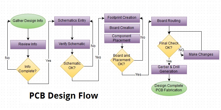 www.homillux.com
PCB Process Flow Chart | www.homillux.com
The Breadth And Depth Of Your PCB Design Workflow
 resources.altium.com
The Breadth and Depth of Your PCB Design Workflow
INFOGRAPHIC: PCB Design Workflow - Design And Layout - SierraConnect
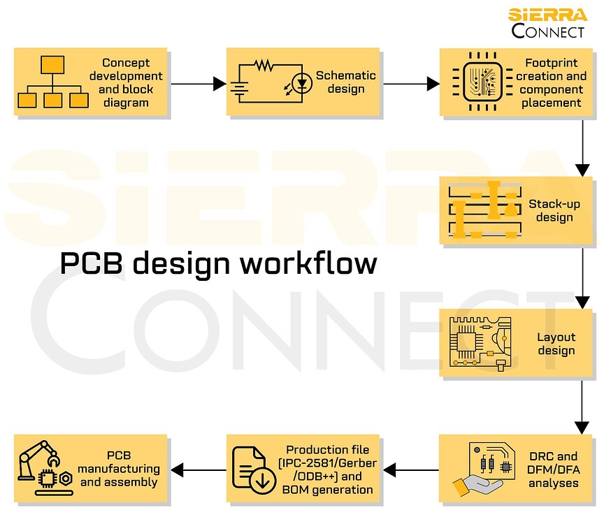 sierraconnect.protoexpress.com
INFOGRAPHIC: PCB Design Workflow - Design and Layout - SierraConnect
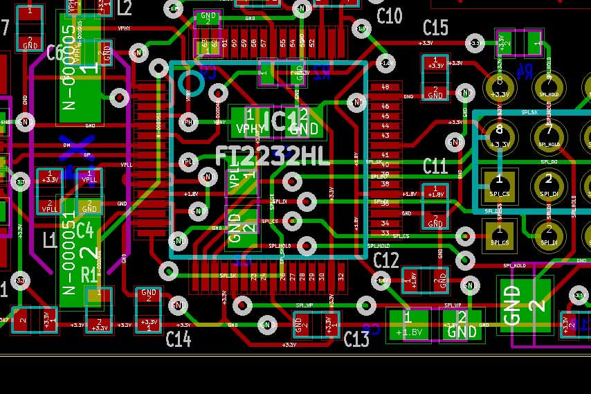
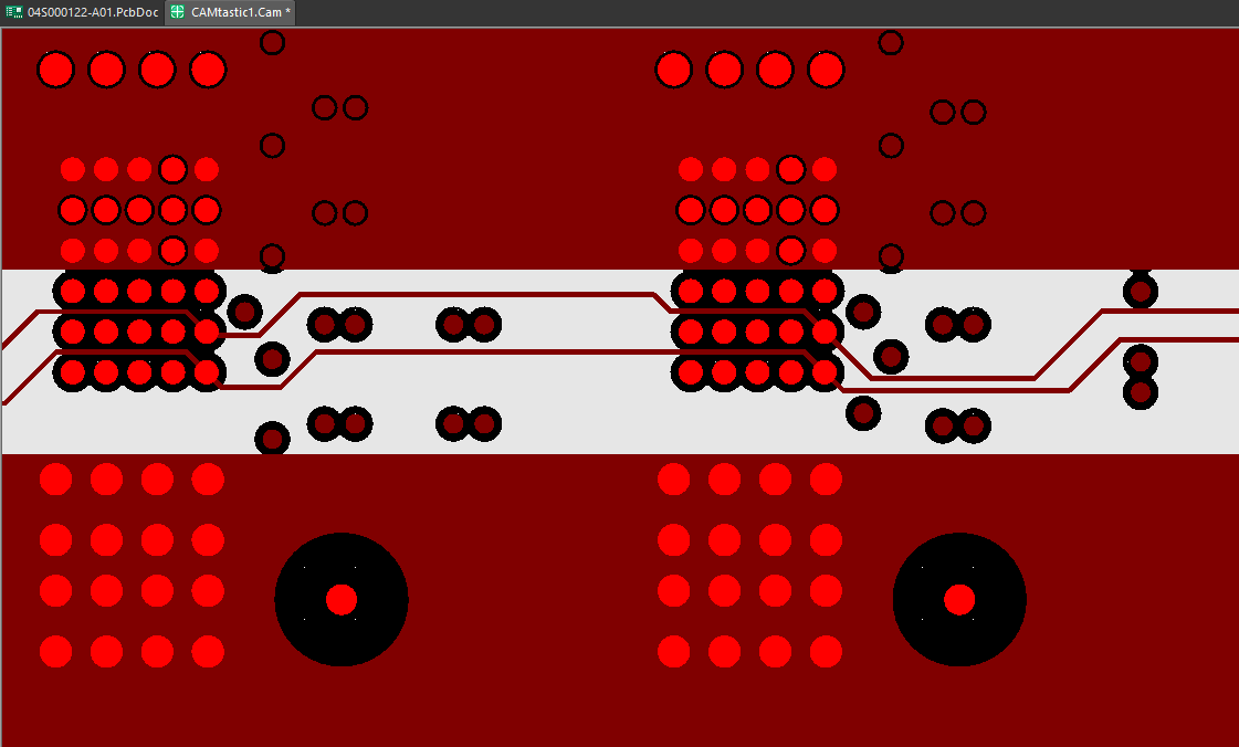
Altium Gerber Output: A Comprehensive Guide – Hillman Curtis: Printed
 hillmancurtis.com
Altium Gerber Output: A Comprehensive Guide – Hillman Curtis: Printed ...
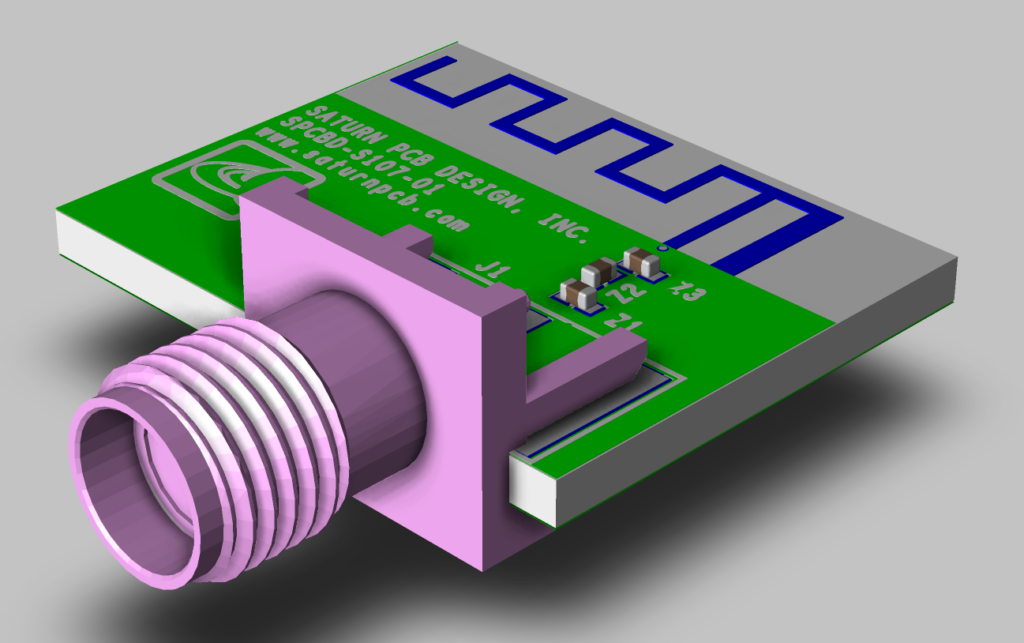
How To Design A PCB Antenna?
 www.nextpcb.com
How to Design a PCB Antenna?
How To Design And Simulate PCB Antenna
 www.fedevel.com
How to Design and Simulate PCB Antenna
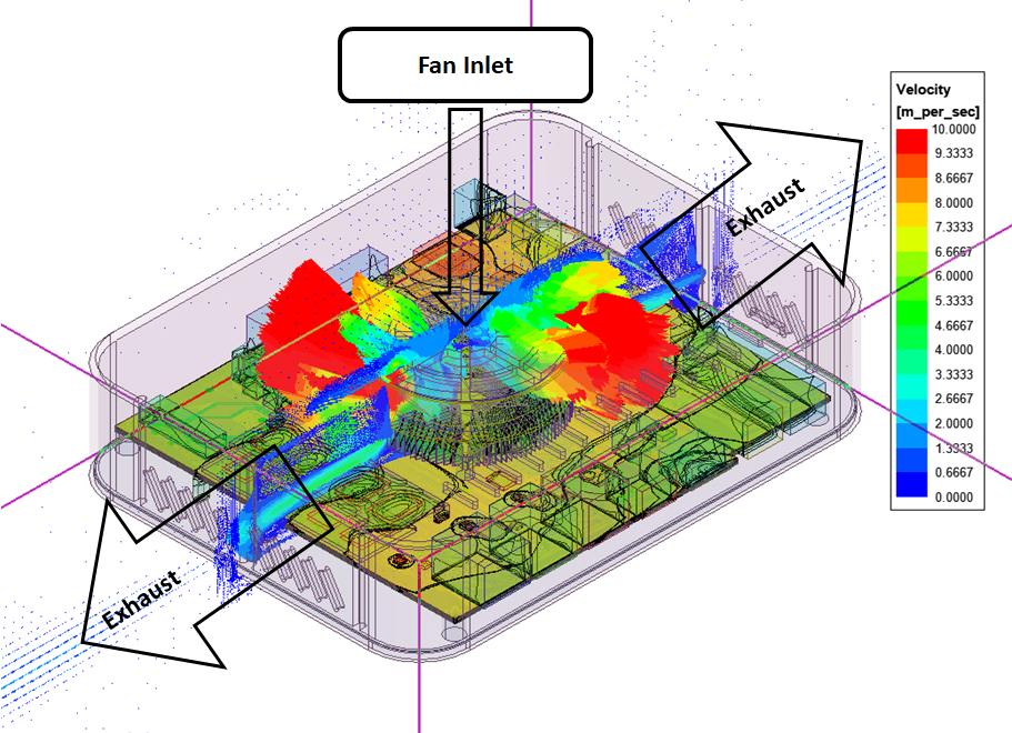
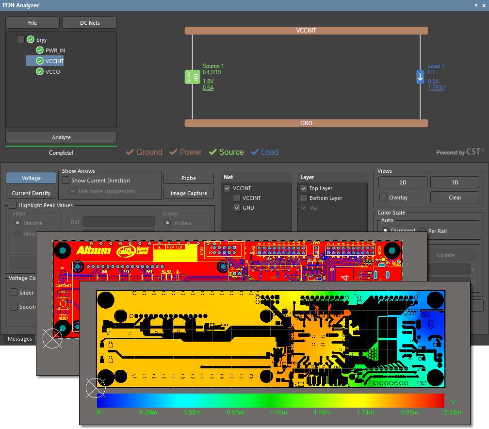
Using PCB Thermal Simulation And Analysis Software In Your Design
 resources.altium.com
Using PCB Thermal Simulation and Analysis Software in Your Design ...
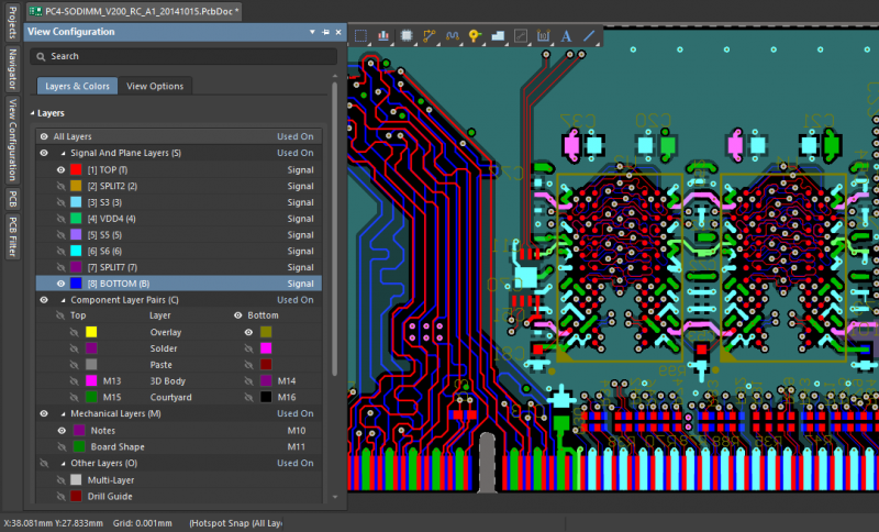
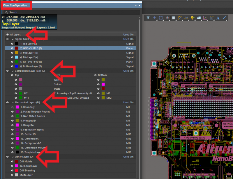
How To Use Altium In Pcb Design At William Melendez Blog
 storage.googleapis.com
How To Use Altium In Pcb Design at William Melendez blog
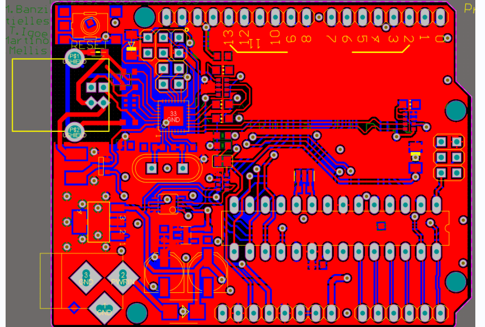
Basic Steps To Design A PCB Layout – PCB HERO
 www.pcb-hero.com
Basic Steps to Design a PCB Layout – PCB HERO
The Best PCB Antenna Design Software Eases Antenna Implementation
 resources.altium.com
The Best PCB Antenna Design Software Eases Antenna Implementation
Using PCB Thermal Simulation And Analysis Software In Your Design
 resources.altium.com
Using PCB Thermal Simulation and Analysis Software in Your Design ...
Build Your Next LED PCB Design In Altium's Unified Environment
 resources.altium.com
Build Your Next LED PCB Design in Altium's Unified Environment
Your Guide To Gerber File Extensions In PCB Design | Blog | Altium
 resources.altium.com
Your Guide to Gerber File Extensions in PCB Design | Blog | Altium
Military PCB Assembly And Workflow In Altium Designer
 resources.altium.com
Military PCB Assembly and Workflow in Altium Designer
Design Rule Checking In PCB Design Workflow: Step-by-Step Guide
 www.fs-pcba.com
Design Rule Checking in PCB Design Workflow: Step-by-Step Guide
Logiciel Gerber PCB - Altium
 www.altium.com
Logiciel Gerber PCB - Altium
Altium Schematic To Pcb
 amusetzxxllibguide.z14.web.core.windows.net
Altium Schematic To Pcb
GSM PCB Antenna: The Ultimate Networking Solution – PCB HERO
 www.pcb-hero.com
GSM PCB Antenna: The Ultimate Networking Solution – PCB HERO
Une Visionneuse Gerber De Premier Ordre | Altium
 resources.altium.com
Une visionneuse Gerber de premier ordre | Altium
Use A PCB Gerber Viewer To Inspect Your Fab Files In Altium 365
 resources.altium.com
Use a PCB Gerber Viewer to Inspect Your Fab Files in Altium 365
Use A PCB Gerber Viewer To Inspect Your Fab Files In Altium 365
 resources.altium.com
Use a PCB Gerber Viewer to Inspect Your Fab Files in Altium 365
How to review your pcb layout & gerber file for rf performance. Logiciel gerber pcb. Your guide to gerber file extensions in pcb design